Designing and testing a new 5V BEC
The KiCad enjoyer has logged on

A few years back, I tried my hand at PCB design for the first time with a small 5V BEC. Although these regulators are common and cheap to buy, it seemed like an easy first step into electronic design. I made a basic design intended for load up to 5V/3A continuous, with PCB mounted XT60-PW connectors to allow passthrough battery voltage. This would allow the BEC to be quickly and easily installed in an exisitng robotics platform. I had the bare PCBs fabricated and then assembled the boards myself by using a frying pan full of sand to reflow the board, which was trickier than I expected thanks to the 0402 components I had included in the design.
The design was reasonably successful and I still use a few of the boards today, but they did struggle to reliably output power at the higher end of the design load. So I decided to take another crack at a passthrough 5V BEC to see how I could improve the design.
Designing
I searched for potential switching regulator ICs to use in this design with a bit more capability than the TI LMR51430 that I used in my previous design. The Analog Device MAX2040x series of regulators seemed promising, with several options available up to a maximum load of 6A and switching frequency of 3 MHz. These regulators can also be used in a multiphase arrangement, where two regulators with their outputs joined and synchronised can share the output load to either reduce the load on either single regulator or combine them to allow a higher total load to be output.
I opted for the MAX20406FOE, with a maximum 6 A output and a switching frequency of 3 MHz. Increasing the switching frequency of a switching regulator reduces the size of the inductor required, which reduces the overall board size. I tried to keep the design simple whilst retaining all the diagnostic output pins of the regulators for use if required in the future. To this end, I kept all the surface mount components on the front face of the board and avoided using components smaller than 0603 size, as well as using the minimum number of unique passive components where possible. The IC manufacturer provides suggested PCB layout to minimise EMI which I followed as far as possible, placing the two regulators adjacent to each other with matching layouts. I also followed the suggested component sizing for the capacitors and inductors. The PCB has 4 layers, and the stackup is Ground/Signal/Power/Ground with the front face also including power to the regulator inputs, and both external faces hosting miscellaneous signal traces.

 Front face of the board with regulator layout
The potential to design the board to make use of the multiphase operation but keep the option of using the two regulators separately was intriguing. The datasheet details the requisite trace layouts for both modes, so I used the rear face of the board to connect these outputs with optional solder joiners. This allows the user to connect the solder jumpers in different configurations depending on how they would like to use the outputs.

 Rear face of the board, showing the solder jumpers and diagnostic solder pads
I kept the passthrough XT60-PW connectors of my first design, so the BEC can still be easily installed and used in an existing robotics platform. I modified the footprint to include a dedicated pad for bare wire to be soldered in place of XT60-PW connectors, and added through hold slots to fit cable ties to provide cable relief if required. On the rear face I exposed the copper between input and output to allow a large solder bridge to be added to support higher passthrough currents. The positive passthrough voltage is also connected on all board layers and stitched with in-pad vias. The main output connector supports a standard 2x2 2.54 mm pitch pin header, and the reverse side of the board has some small solder pads for output monitoring or small loads.
 Input and output power cables directly soldered to the board, making use of the cable relief
 Left - original BEC design, Right - new BEC design, both with XT60-PW connectors
Testing
There were a lot of tests I wanted to run to characterise the performance of the design, but a lot of them require test equipment that I don’t have access to or the resources to acquire. This includes output EMI performance, thermal performance, and output response to passthrough transients to name a few. I did however manage to borrow a variable electronic load to see how the BEC performed against different output step loads. The electronic load was single channel and could operate in constant current mode, where the BEC output is loaded at a continuous current and the voltage monitored. It also supports datalogging of the voltage, current, and power of the BEC output during testing at up to 10 Hz. Although I was using the RS PRO branded version of the KEL-103, the Korad PC control software worked perfectly well, as I assume it is a rebadged version of this unit for RS.
The general test procedure was to increase the desired current draw in steps between a minimum and maximum value, holding each current step for several seconds before incrementing. The output voltage response to these current loads was recorded.
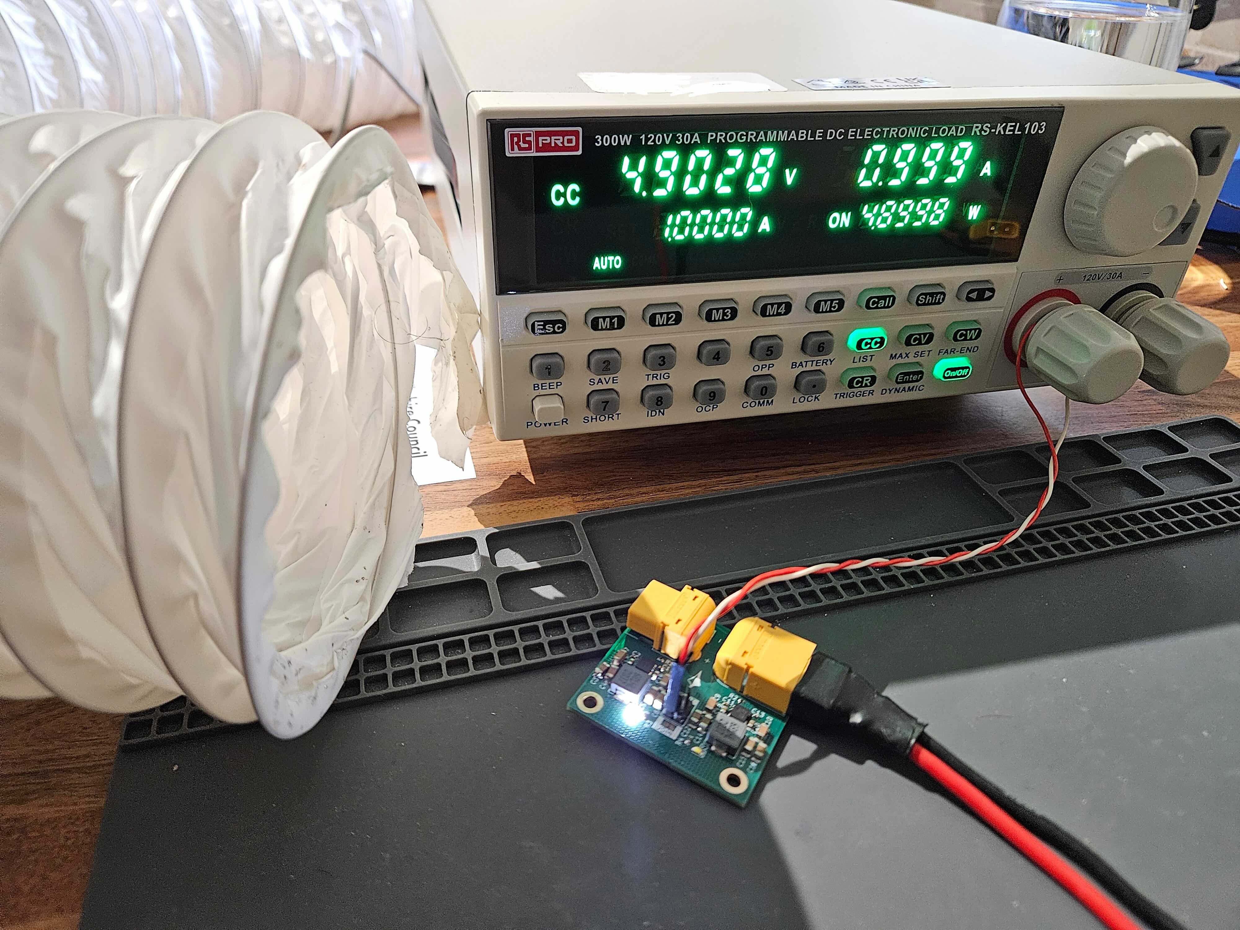 Test setup with electronic load and extraction
Old Design
I took the opportunity to first test my old LMR51430 design as a baseline. It was expected to reach a maximum reliable output of 3 A continuous current. As seen below, once the current draw increases above 2.5 A, the output immediately becomes unstable and unusable. At 2.5 A, the BEC produces a 4.72 V output. The issues seen with reliably powering a Raspberry Pi were likely due to the voltage sag at higher loads.
 Old design, loaded 1-3 A with an increment of 0.5 A and a step duration of 10 seconds
I retested the higher current draws between 2.5 and 3 A with a smaller increment to see where the failure occured. As seen below, the BEC continues to perform to 2.6 A output.
 Old design, loaded 2.5-3 A with an increment of 0.05 A and a step duration of 5 seconds
New Design
I tested my new design in both configurations described earlier. First, the single regulator setup, where only a single regulator contributes to the output load, as is common with BECs available on the market. I repeated the test above from a current of 1 to 6 A but with an increment of 1 A and a duration of 1 minute between increments. Below the results show that the regulator output was stable at all loads up to and including the design maximum of 6 A, with the output voltage reducing to 4.51 V at this load.
 New design, single regulator, loaded 1-6 A with an increment of 1 A and a step duration of 60 seconds
I re-ran the test at the high end of current draw to see how high the BEC could output before becoming unstable. It could output 6.5 A at a voltage of 4.45 V, but became unstable above this.
 New design, single regulator, loaded 4-8 A with an increment of 0.5 A and a step duration of 10 seconds
Next, I tested the multiphase mode or operation, where the two regulators share a combined output. I repeated the first test above and the BEC achieved an output of 6 A at a voltage of 4.49 V. However, after about 20 seconds the output became unstable.
 New design, dual regulators, loaded 1-6 A with an increment of 1 A and a step duration of 60 seconds
I retested the higher end of current draw. The last stable result was 5.8 A and 4.49 V.
 New design, dual regulators, loaded 5-6 A with an increment of 0.05 A and a step duration of 5 seconds
Results
The results of the dual mode were quite underwhelming. Not only did the output fail at 6 A compared to the 6.5 A achieved with the single regulator configuration, but it wasn’t able to output any higher than this despite theoretically being able to support up to 12 A with the load sharing feature. The single regulator configuration was quite successful however, remaining stable up to the design current as expected.nThe output voltage reduction to about 4.5 V under high load was expected but I didn’t think it would drop by 10%, and this will likely not be suitable for high load 5V devices which may brown out at 4.5 V.
The design should be ample for medium load 5 V devices, as the voltage drop is only about 5% (~4.75 V) with a 3 A load. The regulator is setup to use its internal voltage divider for output voltage reference, which is fixed to 5 V. However, there is the option to use an external divider for output voltage references up to 10 V, so this could be used in a future design to bias the output to 5.3 V which would keep the output at or above 5 V for medium load devices and possibly even higher loads. Most 5 V devices are capable of operating on up to 5.3 V.
More Testing
I intended to perform a soak test to assess the thermal performance and stability of the design for long-duration continuous loads, but without a suitable method of recording the temperatures I have skipped this test for now.
The dual regulator configuration has the possibility to provide a single output with redundancy - if one regulator fails, the other should take on the load and maintain the output, for loads up to 6 A. This is not the intended function of the dual phase mode but it would be useful functionality if the working regulator still operated in this way. I’ve not tested this yet but it’s something I want to try soon.
Improvements
For a next iteration of a BEC using these MAX2040x regulators, there are several changes I would make based on these results.
- Consider a compact single regulator design - as the single regulator configuratiuon showed excellent potential, and without the circuitry required for the seconed regulator the design can be shrunk quite considerable and the cost reduced likewise
- Try a hardwired, multiphase, 2-sided assembly design - removing the solder bridges and more closely following the reference design for multiphase operation could improve the performance above 6 A.
- Alternate interfaces - perhaps add an XT30-PW input and output connector for more flexibility.
- Review LED choice - the output LEDs are currently very bright and could be respecified to reduce the brightness.